|
|
|
 |
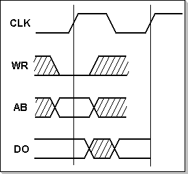 |
FIG.1. Memory read cycle |
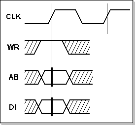 |
FIG.2. Memory write cycle |
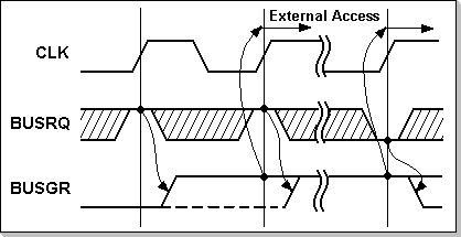 |
FIG.3. Bus request cycle |
The bus grant can be asserted right after
the first active clk transition that finds busrequest asserted, or with
a one-cycle delay; the latter can occur if the busrequest was activated
during the first cycle of a two-cycle instruction.
The first clock active transition that finds the busgrant signal
asserted can be used to strobe the address/wr/(data-in) for an external
access (i.e. it is the beginning of an external RAM-rd or RAM-wr cycle)
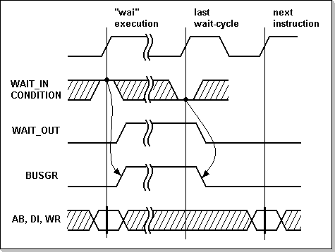
FIG.4. wait instruction when wait-condition is true at the time of "wai" execution (busrq = cleared)
If by the time the "wai" instruction is
executed the wait condition is true, a wait-cycle will be inserted at
the ending of the "wai" instruction. Similarly, for as long as the
beginning of a wait-cycle the wait condition holds true, another
wait-cycle will be inserted.
During the wait-cycles, the busgrant signal is asserted signifying that
the wait-cycles can be used for external (non-DSP) accesses
The wait-out is simply a flag signal asserted during the execution of a
"wai" instruction and during wait-cycles (it is not related to the
busgrant signal).
Because the "wait-out" signal is not asserted prior to the "wai"
execution, it cannot be used as a wait-condition setup signal (the wait
condition is checked on the "wai" leading clock edge, at which time the
"wait-out" is not yet asserted).
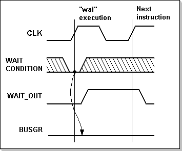 |
FIG.5. Wait instruction when the wait condition is false at the time of "wai" execution (BUSRQ = clear) |
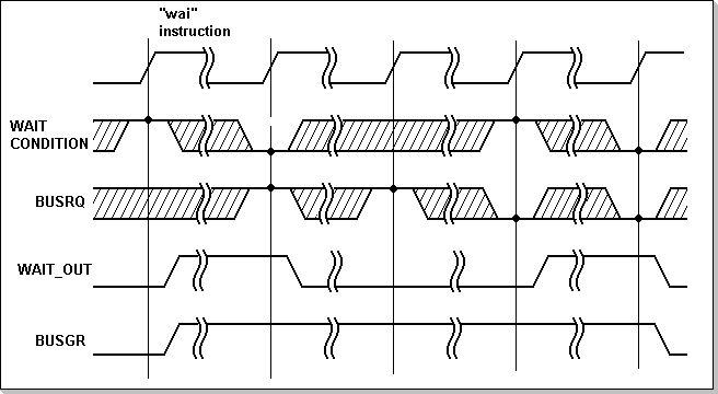
FIG.6. Interaction between bus requests and wait condition during the execution of a wait instruction
- At the beginning of a "wai" instruction execution the wait-condition control has priority over busrq in the sense that it forces the addressing state machine into the wait-cycles modes
- Once in one mode (wait-cycles or busrequest acknowledge) the state machine does not change state while the corresponding control signal (busrq/wait condition) stays unchanged.
- Each time the addressing state machine exits one of the wait-cycles or busreqest acknowledge states, it checks for the "other" control signal before proceeding to the next instruction (i.e. a "wai" instruction can be interrupted by bus request the moment the wait condition becomes false, and then the "wai" can be <<reexecuted>> if the condition is again true by time busrequest is cleared.
In the previous descriptions the wait-condition signal represents an internal processor signal derived from the processor wait_in input and a "wai" instruction argument. The wait-condition is obtained by logical "and" between the wait input and the "wai" argument. This way individual bits from the wait_in input can be checked, or a group of bits can be tested simultaneously.
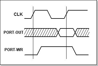 |
FIG.7. Data port-output cycle ("lds.com") |
The data port output cycle occurs one
clock cycle after the (first cycle of the) actual "lds.com" instruction
execution (the instruction can become multi-cycle if extended by a
busrequest).
The port’s output data remains unchanged until the execution of the
next "lds.com" instruction.
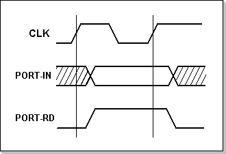 |
FIG.8. Data port -input cycle ("sts.com") |
The execution of a "sts.com" instruction
is signaled by asserting the port_rd output; after this signal becomes
active, a stable value must be placed on the port_in bus. The port_rd
can be used to setup a value on port_in (i.e. port_in is not read prior
to the port_rd assertion) as long as the port_in setup time is not
violated (although port_in is strobed on the next active clock cycle
after the port_rd assertion, its setup time is close to one clock
cycle).
If the "sts.com" instruction is extended by a busrequest, only the
first cycle will be a port-read cycle (i.e. the port_rd signal will be
asserted only during the first, non-bus acknowledge, cycle).
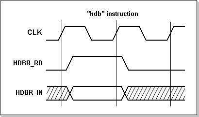 |
FIG.9. Hardware Directed Branch "hdb" execution (assuming no bus requests). |
When a "hdb" instruction is executed, the
processor jumps at a ProgramROM address that is derived from the
hdbr_in input bus (the actual target address is obtained by adding the
value present on the hdbr_in bus with a hardware-defined constant).
The execution of the first cycle of a "hdb" instruction is signaled by
asserting the hdbr_rd output; after this signal becomes active, a
stable value must be placed on the the hdbr_in bus. The hdbr_rd can be
used to setup a value on hdbr_in (i.e. hdbr_in is not read prior to the
hdbr_rd assertion) as long as the hdbr_in setup time is not violated
(although hdbr_in is strobed on the next active clock cycle after the
hdbr_rd assertion, its setup time is close to one clock cycle).
If the "hdb" instruction is extended by a busrequest, the hdbr input
will only be read during the first instruction cycle (i.e. the bus
acknowledge cycles are inserted at the end of the instruction, after
its second clock cycle).
The processor is featured with asynchronous Reset and synchronous Restart controls.
The Reset signal is the processor’s global
asynchronous reset. After Reset, the processor starts executing the
instructions at ProgramROM address 0, and the registers are affected as
follows: the hardware loop ("rpt" instruction) -related registers and
the processor status register "psr" are reset; the conditional branches
condition-chaining flag is reset. All other processor registers will be
considered to be undefined after Reset.
The Reset signal has to be maintained active for at least 4 active
clock transitions.
The Restart signal is similar to Reset,
but it is a synchronous signal; the processor registers are affected
the same way as in the case of Reset, but the changes take place on the
first active clock edge that finds the Restart signal asserted.
During the processor Restart sequence (when Restart is asserted) the
bus_grant signal is asserted, signifying that the DataRAM can be
accessed by other modules (during Reset the bus_grant signal is not
asserted). The bus_grant is asserted the moment Restart is asserted,
and it is de-asserted the moment the Restart signal is de-asserted.
The Restart signal must be active for at least 4 active clock
transitions.